
First of all, digital circuits work with 0’s and 1’s (i.e. bits). Numbers are therefore represented in binary before they can be added in the digital circuits that we are going to design. For now, let’s assume numbers are non-negative \(X = 0, 1, 2, \ldots\) so that a simple binary conversion suffices, for instance:
\[X = 9_{10} = 1001_{2}\] \[Y = 4_{10} = 0100_{2}\]We add digit by digit from the least significant end (right hand side) through to the most significant end (left hand side), with possibly a carry between digits. If we denote each bit of number \(X\) as \(X_i\), then we need a circuit to add bits \(X_i\) and \(Y_i\) with a carry in \(C_i\). And the circuit produces a sum bit \(S_i\) and a carry out bit \(C_{i+1}\), which is the carry in bit for the next digits.
The Full Adder
The behaviour of the circuit that adds the bits can be easily listed in a truth table:
| \(C_i\) | \(X_i\) | \(Y_i\) | \(C_{i+1}\) | \(S_i\) |
|---|---|---|---|---|
| 0 | 0 | 0 | 0 | 0 |
| 0 | 0 | 1 | 0 | 1 |
| 0 | 1 | 0 | 0 | 1 |
| 0 | 1 | 1 | 1 | 0 |
| 1 | 0 | 0 | 0 | 1 |
| 1 | 0 | 1 | 1 | 0 |
| 1 | 1 | 0 | 1 | 0 |
| 1 | 1 | 1 | 1 | 1 |
This circuit is called the full adder. And there are several interesting ways to study the truth table:
- The first four rows are the cases when the carry in is 0. Extracting these rows without the first column gives you the truth table of the half adder that adds two bits and gives a sum bit and a carry bit.
- The output column \(C_{i+1}\) is counting two or more 1’s while the output column \(S_i\) is counting odd number of 1’s.
- \(S_i\) and \(C_{i+1}\) are two different functions of our input bits \(X_i\), \(Y_i\) and \(S_i\).
Based on the second point above, we can derive simple Boolean equations for \(S_i\) and \(C_{i+1}\):
\[\begin{align} S_i &= AB + AC + BC\\ C_{i+1} &= A \oplus B \oplus C\\ \end{align}\]If you are not familiar with exclusive OR gate as denoted by \(\oplus\) you can check it out here.
Let’s give a symbol for the full adder to help our following discussion.
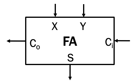
The arrows indicate the flow of the input bits, carry bits and the sum bits. And when there is no ambiguity the labels for the inputs/outputs are skipped in the following diagrams.
The Ripple Adder
The full adder is the circuit/device to handle addition of two bits so the remaining job is to connect the carries together, forming a chain along a list of full adders. For example, a 4-bit ripple adder is like this:
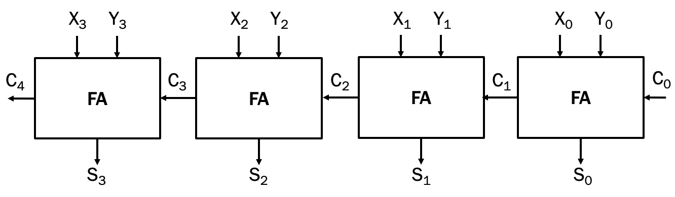
The design can be easily extended for as many bits as you want. You just need to append more full adders to the end of the chain. The more significant bits are on the left of the diagram so it matches our convention on paper. We also call this design iterative as it can be used repeatedly to construct bigger circuits for the same operation.
This gives the standard ripple adder which is used so many digital systems that involves additions and subtractions. It is imperative to note that the size (or width) of the adder, \(N\) has to be decided at the time when the adder is built because the adder cannot be extended easily once it sits in the system (unless you are using programmable logic devices like FPGAs). As a result, the rule of thumb is to estimate the order of your calculations and make the adder big enough. For instance, if you intend to add numbers in a thousand range then you probably need an adder of 10-12 bits wide.
When \(X\) and \(Y\) are non-negative (i.e. unsigned), a carry out from your last full adder (e.g. \(C_4\) in the diagram above) indicates an overflow of the \(N\)-bit adder. You can save the carry to preserve the correct sum or simply raise an error as you cannot go on with further additions.
For now, addition is sorted, but how about subtraction? In the next blog, I will discuss the modification required to turn a ripple adder into a subtractor using the useful 2’s complement representation.